


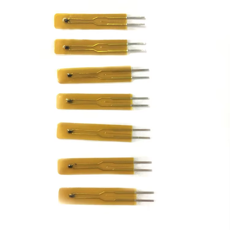
Concepte fundamentale privind funcționarea termistorilor cu film subțire
Precizia măsurării temperaturii datorită proprietăților rezistive NTC
Funcționarea termistorilor NTC este reglementată de principiile semiconductorilor. La temperaturi ridicate, termistorii din oxid metalic, cum ar fi cei care conțin mangan, cobalt, nichel sau oxigen, prezintă o rezistență electrică redusă. Există anumite domenii de temperatură în care rezistența lor scade, așa cum este ilustrat pe o curbă. Această caracteristică le permite să detecteze variații de temperatură mai mici de 0,1 grade Celsius. Termistorii NTC depășesc performanța senzorilor obișnuiți de temperatură, deoarece pot detecta modificări mici ale temperaturii fără a necesita prelucrarea electronică a semnalului. Termistorii cu rezistență ridicată sunt rezistenți la șocurile electrice și termice, ceea ce rezultă din structurile cristaline stabile formate în urma procesării termistorilor la temperaturi înalte (1000–1400 de grade Celsius). Termistorii în strat subțire pot suporta cicluri repetitive de creștere și scădere a temperaturii fără a se deriva semnificativ. Datorită combinației dintre durabilitatea ridicată, rezistența superioară la șoc termic și timpii de răspuns rapizi, termistorii NTC în strat subțire sunt ideali pentru utilizare în aplicații medicale sensibile și în aplicații auto care necesită o fiabilitate ridicată și condiții de mediu variabile.
De ce arhitectura cu film subțire îmbunătățește stabilitatea și timpul de răspuns al TCR
Când se iau în considerare opțiunile cu elemente ceramice sau înfășurate din sârmă, abordarea cu film subțire oferă avantaje incontestabile. Folosind tehnica numită pulverizare catodică (sputtering), producătorii aplică stratul de Mn-Co-Ni-O la o grosime de doar 50–250 de angstromi. Acest lucru conduce la îmbunătățiri semnificative, atât în ceea ce privește uniformitatea, cât și reducerea problemelor legate de limitele de grăunțire ale particulelor individuale. Ca urmare, coeficientul de temperatură al rezistenței este mult mai stabil, variația acestuia fiind de aproximativ 0,5 % în condițiile tipice de funcționare. Filmele sunt, de asemenea, extrem de responsive, având un timp tipic de răspuns de < 100 ms, datorită masei termice reduse a straturilor subțiri. Adăugarea de materiale izolante și flexibile din poliimid permite acestor dispozitive să funcționeze în aplicații supuse vibrațiilor mecanice continue sau ciclărilor termice rapide. Aceasta este fiabilitatea pe care industriile o cer pentru medii de fabricație dificile sau pentru condiții imprevizibile din aplicațiile auto.
Producția termistorilor cu film subțire: Proceduri de depunere și modelare
Aderență optimă: Selectarea substratului și pregătirea suprafeței
La alegerea materialelor, se iau în considerare, cel mai probabil, substraturile din aluminiu și safir, deoarece acestea sunt stabile din punct de vedere termic, asigură o izolare electrică adecvată și sunt compatibile cu filmele de oxid metalic. Înainte de orice etapă de depunere, pregătirea suprafeței (în cazul substraturilor din aluminiu) este de o importanță absolută. Suprafața este pregătită prin curățare ultrasunet, urmată de gravare cu plasma de oxigen, o procedură care asigură o rugozitate de sub 5 nanometri. Aceasta este importantă deoarece unul dintre mulții factori care influențează aderența este rugozitatea suprafeței, iar o suprafață mai netedă conduce la o aderență mai bună; s-a demonstrat că procedura de pregătire a suprafeței descrisă mai sus poate reduce cu 70% apariția delaminației pe suprafața pregătită în timpul ciclărilor termice, un factor de mare importanță în cadrul acestor ciclări termice.
Sputterarea ca metodă preferată pentru depunerea termistorilor sub formă de film subțire Mn–Co–Ni–O
Sputterarea magnetron reactivă este metoda cea mai fiabilă de sinteză a filmelor subțiri Mn-Co-Ni-O, asigurând în același timp stoechiometria solicitată. Această metodă implică controlul precis al atmosferei din camera de sputterare, folosind amestecuri de gaze argon și oxigen, permițând filmului subțire să mențină o precizie stoechiometrică de aproximativ 1,5%, în timp ce se obțin simultan viteze de depunere de aproximativ 0,2 µm/min. Când cercetătorii optimizează distanța dintre materialul țintă și suprafața substratului, se înregistrează o scădere a numărului mediu de defecțiuni și o creștere semnificativă a coeficientului de temperatură al rezistenței (TCR) uniform al filmului. În comparație, filmele obținute prin metode de evaporare termică sunt semnificativ mai puțin dense și prezintă o aderență redusă la substrat. De fapt, testele independente au arătat că filmele subțiri create prin sputterare au o densitate a materialului cu până la 40% mai mare, ceea ce reprezintă un indicator esențial pentru abordarea defecțiunilor și încurajează utilizarea sputterării în aplicații dense din numeroase domenii.
Modelarea precisă a termistorilor cu film subțire folosind fotolitografie și gravare
Fotolitografia de înaltă precizie permite fabricarea electrozilor și a structurilor senzoriale la scară micrometrică, cu detalii până la 10 microni. Odată ce este atins acest nivel de rezoluție, efectuăm aplicarea prin centrifugare a unui fotoresist, urmată de expunerea fotolitografică prin măști de crom și dezvoltarea fotoresistului. Pasul ulterior constă în gravarea umedă cu soluție de clorură ferică pentru îndepărtarea întregului material termistor care nu este acoperit de mască. Acest proces asigură o precizie dimensională de ± 0,8 microni. În majoritatea cazurilor, acest nivel de precizie este necesar deoarece nivelurile de rezistență ale senzorilor pot fi afectate chiar și de cele mai mici variații din matricile dense de senzori. Calitatea modelului senzorului determină calitatea senzorului și modul în care acesta răspunde la modificările termice, precum și variabilitatea răspunsului senzorului în timpul funcționării.

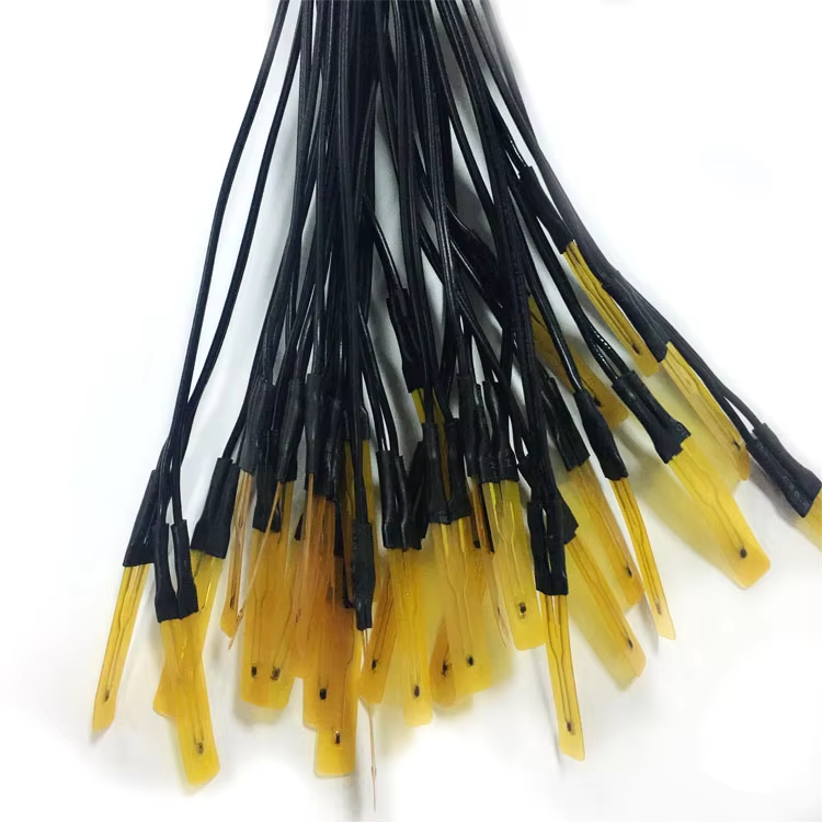
Integrarea electrozilor și ingineria interfeței pentru fiabilitate pe termen lung
Electrozi Ni–Cr și Pt: Prevenirea difuziei și asigurarea stabilității contactului ohmic
O atenție corespunzătoare acordată modului în care sunt integrate electrozii joacă un rol esențial în atenuarea degradării interfețiale, una dintre principalele cauze ale problemelor de deriva pe termen lung. De exemplu, aliajele de nichel-crom servesc ca bariere eficiente la difuzie, deoarece împiedică difuzia cationilor din electrozi către regiunile nedorite ale stratului de termistor. În plus, electrozii de platină prezintă avantaje datorită rezistenței lor scăzute și stabilității contactelor, chiar și după numeroase cicluri termice. O abordare inginerească pentru îmbunătățirea adeziunii interfețiale și minimizarea reacțiilor nedorite constă în aplicarea unor tratamente la scară atomică, cum ar fi oxidarea controlată și curățarea suprafeței prin fascicul de ioni. Proiectarea straturilor interfețiale a demonstrat că reduce deriva potențialului de contact la sub 0,5 ohmi după 10.000 de cicluri termice și diminuează tensiunea interfețială cu 40 % față de metalizarea anterioară. În final, toate aceste măsuri vor îmbunătăți precizia măsurătorilor, de la începutul utilizării dispozitivului până la uzura completă a acestuia.
Prelucrarea termistorilor cu strat subțire, cu asigurarea calității și evaluarea performanței. Asigurarea calității și metodele de control al calității utilizate în prezent pentru termistorii cu strat subțire s-au dovedit extrem de eficiente și repetabil fiabile în îndeplinirea unor niveluri excepționale de fiabilitate și precizie. Efectuăm cicluri termice între +125 °C și -40 °C, pe o perioadă de peste 1000 de cicluri, pentru a evalua integritatea structurală și rezistența. Pentru testele de derivație pe termen lung, îmbătrânirea accelerată presupune expunerea eșantioanelor la o temperatură de 85 °C și o umiditate relativă de 85 %, timp de peste 1000 de ore, pentru a garanta că derivația rămâne sub 1 %. În ceea ce privește testarea electrică, efectuăm o hartă completă a valorilor coeficientului de temperatură al rezistenței (TCR) și testăm interferența electromagnetică, pentru a asigura menținerea unei precizii de ±0,1 °C pe durata de funcționare. Fiecare dintre procesele noastre de producție este supus unui control statistic riguros al procesului, pentru a monitoriza variația grosimii stratului de 5 nanometri și alinierea electrozilor, utilizând funcții automate de aliniere optică. Imagistica termică în timp real, efectuată în timpul tăierii cu laser, captează detalii microscopice (la scară de microni), iar testele de încălzire preliminară (burn-in) elimină componentele care prezintă defecte precoce. Toate aceste teste și activități de monitorizare asigură faptul că termistorii noștri ating o durată de funcționare operațională de 100.000 de ore în condiții extreme de solicitare performantă, fără apariția unor defecțiuni.
Întrebări frecvente
Care este avantajul principal al termistorilor NTC?
Termistorii termici NTC sunt dispozitive destul de simple, dar avantajele lor sunt remarcabile. Avantajul principal este că termistorii NTC prezintă un grad considerabil de stabilitate pe perioade lungi de timp și pot fi compensați cu o precizie de 0,1 grade Celsius.
Care este diferența principală dintre termistorii în film subțire și ceilalți?
Termistorii în film subțire sunt realizați cu un strat foarte subțire de Mn-Co-Ni-O și oferă, astfel, o uniformitate mult mai bună, o răspuns temporal mai rapid și, în general, o înlocuire mai bună a materialelor ceramice sau înfășurate în fir.
Care este impactul pregătirii suportului în procesul de fabricare al termistorilor?
O pregătire corectă a suportului îmbunătățește aderența oxizilor metalici la suport, reducând astfel probabilitatea separărilor straturilor legate de testare cu aproximativ 70%. Straturile netede sunt mai capabile să reziste separărilor legate de testare.
Ce efect au electrozii Ni-Cr și Pt asupra termistorilor?
Electrozii Ni-Cr și Pt sunt menționați în interiorul termistorilor deoarece Ni-Cr oferă o barieră împotriva difuziei, iar Pt asigură un contact stabil și de joasă rezistență. Este combinația celor două care reduce deriva în timp și îmbunătățește stabilitatea contactului în cadrul ciclurilor repetate.

